Precision ITO Coating Technology Solutions


Star-Optics specializes in precision Indium Tin Oxide (ITO) thin film coatings deposited on optical glass, fused silica, and polymer substrates. Using advanced magnetron sputtering and vacuum deposition technology, we deliver high-uniformity transparent conductive coating with precisely controlled ITO film thickness and ITO sheet resistance tailored for touchscreen panels, optical sensors, display systems, smart windows, solar cells, and EMI shielding applications.

Our custom ITO coating process ensures reliable electrical conductivity while maintaining superior optical transmittance across visible and near-infrared wavelengths.

Applications of ITO Conductive Coatings

Our ITO conductive coatings are engineered for reliable performance in the following key applications:

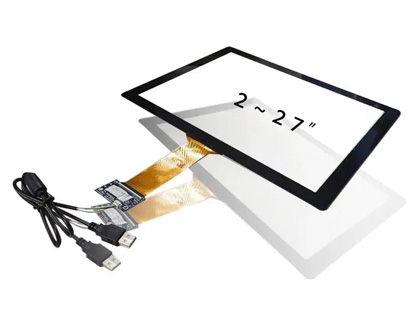
Touchscreen Panels & Capacitive Touch​

ITO coatings with 30–80 Ω/sq sheet resistance and >90% transmittance ensure uniform surface conductivity for accurate capacitive touch response while maintaining excellent visual clarity. Our high transparency conductive glass minimizes color distortion and supports multi-touch functionality.

Photovoltaic & Solar Cells

Optimized ITO coatings maximize photon collection efficiency while maintaining excellent conductivity for current extraction. Our custom ITO coating designs reduce parasitic absorption to preserve solar cell efficiency.

Optical Sensors & Imaging

Customized precision ITO thin film coatings for light-sensitive applications, where low resistance ITO layer design balances electromagnetic shielding with minimal optical absorption. Ideal for image sensors, UV detectors, and thermal imaging windows.

We provide rapid turnaround on custom specifications and technical consultation to ensure your precision ITO thin film meets exact performance targets.

Custom ITO Glass Fabrication and Processing Capabilities

Comprehensive Machining Capabilities 

We provide full-process customization, including cutting, etching, drilling, edge grinding, chamfering, scribing, and slotting, to meet diverse design and functional requirements.

Precision Cutting with Smooth Edges 

High-accuracy processing ensures clean edges, minimal chipping, and excellent dimensional consistency across large or thin substrates.

Stable Coating Uniformity

Each ITO film is deposited with tight control of thickness and sheet resistance, maintaining consistent performance across the entire surface.

Accurate Sheet Resistance Measurement

ITO conductivity is verified using a four-point probe tester, ensuring precise and repeatable measurement of surface resistance for every coated substrate.

Star-Optics provides one-stop ITO coating services specifically designed for universities, research institutes, and corporate R&D centers. From initial coating deposition through final component delivery, we handle every stage of production—including precision cutting, etching, drilling, edge polishing, beveling, scribe marking, and custom slot machining—ensuring components meet exact specifications for laboratory research and commercial applications.

Understanding ITO Coating Technology

ITO Coating Working Principles

  1. Electron Conduction –
    The indium–tin oxide layer forms a continuous conductive network, allowing free electrons to move across the surface while maintaining visible light transparency.

  2. Producing ito glassOptical Transparency –
    The thin ITO layer (typically 10–200 nm) and the SiO₂ buffer layer are optimized to minimize optical reflection and absorption within the visible wavelength range.
  3. Thin Film Deposition Control –
    Using magnetron sputtering, ITO is deposited under high-vacuum conditions with precise control of film thickness and uniformity. This ensures stable sheet resistance and consistent optical performance.

  4. Surface Tuning & Annealing –
    Post-deposition annealing enhances the crystalline structure and carrier mobility, improving both electrical conductivity and optical transmittance stability.

  5. Etching for Circuit Patterning –
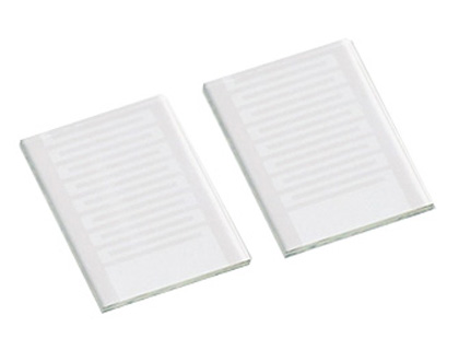
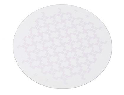
    The ITO layer can be precisely etched to form conductive circuits or electrode patterns, allowing integration into touch panels, sensors, and optical-electronic devices. Etching accuracy ensures clean pattern edges and reliable electrical isolation between conductive areas.

Technical Specifications of ITO Coating

*All values represent typical data measured under 550 nm wavelength, 25°C ambient conditions. Film properties can be customized according to target resistance, optical transmittance, and substrate type.

Grade Sheet Resistance (Ω/sq) Film Thickness (nm) Transmittance @550nm (%) Typical Applications
100 ≤100 60–100 ~80 Prototypes, low-conductivity needs
080 ≤80 55–80 ~83 Standard touchscreens
060 ≤60 40–60 ~85 General displays
050 ≤50 35–50 ~88 Sensors, industrial devices
040 ≤40 30–40 ~90 High-performance displays
030 ≤30 20–30 ~92 Premium touch panels
025 ≤25 17–25 ~93 Optical-grade devices
020 ≤20 13–20 ~95 High-transparency applications
017 ≤17 12–17 ~97 Optical instruments
015 ≤15 10–15 ~98 Low-resistance optics
010 ≤10 7–10 ~98 Ultra-low resistance film
007 ≤7 5–7 ~99 Specialized optical systems
005 ≤5 3–5 ~99 EMI shielding, conductive glass

FAQS

What is ITO glass?

Laser cutting is a precise manufacturing process that uses a high powered lasers to cut through various materials, including wood, steel, and certain plastics. The laser beam is generated inside a laser resonator by amplifying light through stimulated emission of radiation, and then directed onto the workpiece using optics such as mirrors and lenses.

Laser cutters are commonly used to create 2-dimensional parts from sheet or plate materials, serving both industrial and hobbyist applications. This versatile technology can process both metallic and non-metallic materials across a range of thicknesses with exceptional accuracy and clean edges.

Sheet resistance (measured in ohms per square, Ω/□) represents the electrical resistance of the ITO coating.

  • Lower values (≤10 Ω/□) are suitable for applications that require strong electrical conductivity such as heaters or EMI shielding.

  • Higher values (30–200 Ω/□) are common for touch sensors, research, and general optoelectronic applications.
    The ideal range depends entirely on the device design and power requirements.

While soda-lime and borosilicate glass are the most common substrates, ITO can also be deposited on:

  • Aluminosilicate glass

  • Quartz and fused silica

  • PET or flexible polymer films

  • High-temperature specialty glass
    Each substrate provides different thermal, optical, and mechanical characteristics.

Yes. ITO coatings can be precision-patterned using laser ablation, photolithography, or chemical etching. Custom geometries such as grids, electrodes, tracks, and micro-features can be created to fit specific optical or electronic designs.

Standard ITO coatings offer 80–90% transmittance in the visible range, depending on film thickness and sheet resistance. Higher conductivity generally reduces transparency slightly, so the two parameters must be balanced.

Contact Us Now